In the fast-paced world of electronics, Printed Circuit Boards in hindi (PCBs) play a pivotal role as the backbone of countless devices we use every day.
These small but mighty boards serve as the foundation upon which electronic components are mounted and connected, enabling the seamless operation of everything from smartphones and laptops to medical devices and automotive systems.
In this comprehensive exploration of Printed Circuit Boards in hindi, we will delve into their history, design, manufacturing process, applications, and the future trends shaping this crucial technology.
A Brief History of Printed Circuit Boards in hindi
The concept of Printed Circuit Boards in hindi dates back to the early 20th century when engineers began exploring ways to streamline the process of connecting electronic components.
Prior to the advent of PCBs, electronic circuits in hindi were constructed using point-to-point wiring, a laborious and error-prone method.
The breakthrough came in the 1940s when a patent was filed for a method of creating an electrical path directly on an insulating board.
This laid the foundation for the modern PCB as we know it today.
Over the decades, advancements in materials and manufacturing techniques have transformed PCBs from simple single-layer boards to complex multi-layer structures capable of supporting high-speed digital signals and intricate electronic designs.
Today, PCBs are integral to nearly all electronic devices, from consumer electronics to industrial machinery, making them an indispensable component of modern technology.
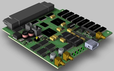
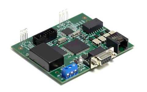
Designing Printed Circuit Boards in hindi: The Art of Miniaturization
The design of a Printed Circuit Board in hindi is a meticulous process that involves careful consideration of various factors such as component placement, signal integrity, thermal management, and manufacturability.
In addition to miniaturization, PCB designers must also optimize the layout of components to ensure efficient signal propagation and minimize electromagnetic interference.
Signal integrity is crucial in high-speed digital circuits in hindi, where even minor impedance mismatches or signal reflections can degrade performance and lead to data errors.
By carefully designing the routing of traces and managing signal paths, designers can ensure optimal signal integrity and reliability in their PCB designs.
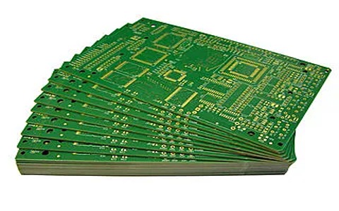
Manufacturing Printed Circuit Boards in hindi: Precision Engineering Meets Innovation.
The manufacturing process of Printed Circuit Boards in hindi is a complex and highly precise operation that involves a series of steps to transform a design file into a functional board.
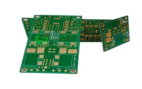
The process begins with the fabrication of the board itself, where a substrate material such as fiberglass or composite is coated with a layer of copper foil.
This substrate serves as the foundation upon which the circuit pattern will be etched.